
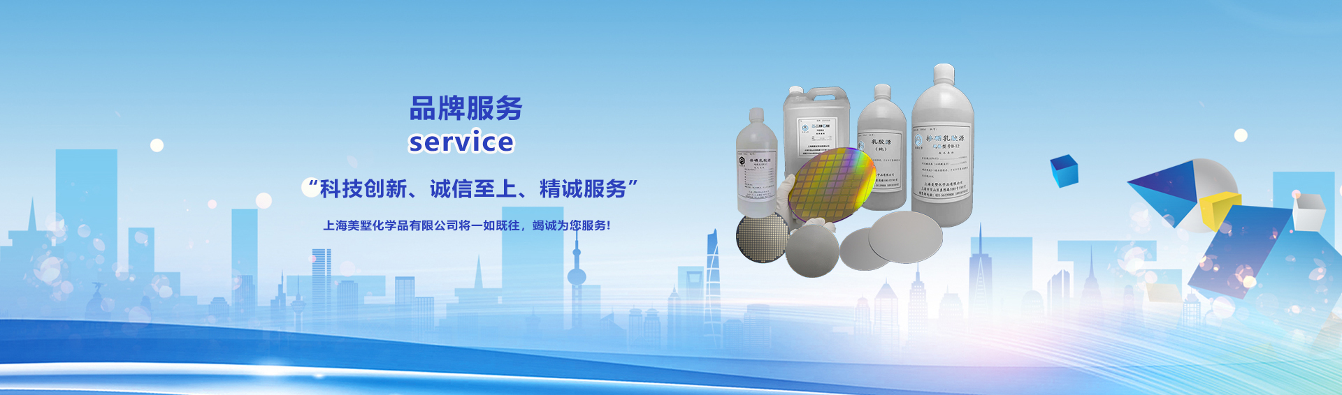
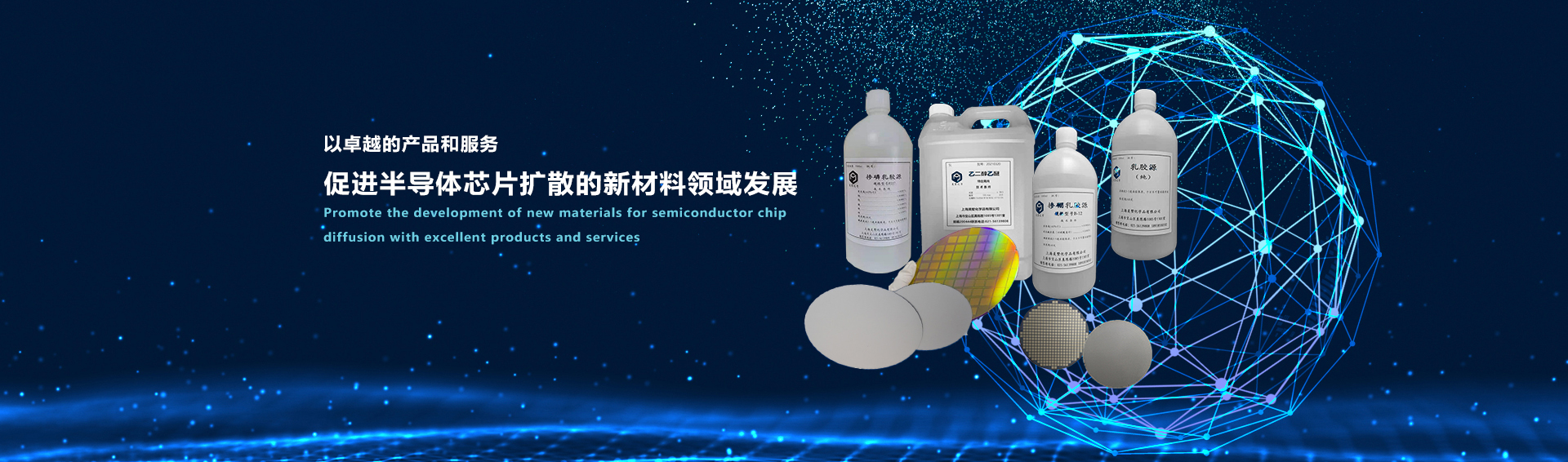
Introduction: semiconductor chip diffusion doping source materials
Introduction to the
This product is not mixed with any doping source, customers can according to the production technology needs of the enterprise, in the latex source can be mixed with phosphorus, boron, arsenic, antimony, aluminum and other certain concentration of impurities, the content of impurities can be adjusted in a larger range;Make it a doped silicon dioxide emulsion, which can be applied to impurity diffusion. Using doped silicon dioxide emulsion, a series of advantages that are not available to other commonly used sources at present can be obtained.
Spread in the silicon wafer surface after the source of latex coating will not damage the surface of silicon, phosphorus source diffusion and there is no such as liquid contamination, such as metaphosphate and clean silicon surface alloy and latex source in the coating and the diffusion of less toxic impurities precipitation, especially with phosphorus arsenic and other toxic substances diffusion source, use latex source is far more convenient than liquid source security,But also can prolong the quartz tube service life and so on.
Phosphorus - doped latex source (semiconductor chip manufacturing: diffusion doping source) new material
Introduction to the
Phosphorus doped latex source new material products, is designed for the diode manufacturing and the development of innovative inventions, mainly used in semiconductor chip diffusion of new materials: won the 16th Chinese scientists forum 2019 China Science and Technology Innovation and Invention Achievement Award, won the 2019(the fifth) Hua ZunAward China business ten industries innovative enterprises:In June 2020, it was authorized by the State Intellectual Property Office for invention patent.
Applications: Diffusion doping sources for semiconductor chips.
Quality effect: the new material of phosphor-doped latex source has been used by customers for more than ten years, and the user reflects the good effect. The diffusion coefficient is relatively concentrated, the chip junction depth is uniform, the phosphorus flower is fine, the silicon wafer surface is clean, the silicon lattice is uniform in thickness, and there is no alloy point.After diffusion, the device surface is clean and dry, which will not damage the silicon surface and is conducive to lithography.
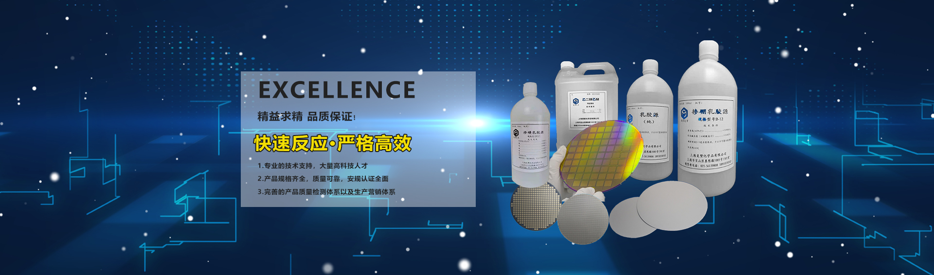
Advantages: simple equipment, few procedures, one step process can be completed diffusion, source concentration can be adjusted in a larger range, the basic non-toxic impurities precipitation, etc., than the current commonly used liquid source, solid source has more advantages, basically non-toxic odorless more environmental protection, than the conventional process is simpler, stable, reliable, safe;At the same time, the diffusion is not affected by airflow. In the same furnace, not only the uniformity of the same large plate is good, but also the uniformity between the plates is good, and the reproducibility of the results is also quite good.
Operation process:
1. Coating method coating source: the use of central rotation coater.Start the motor to start the coating machine, so that the silicon wafer adhesive adsorption plate high-speed rotation, speed of about 3000-4000 RPM, the clean silicon wafer on the adhesive adsorption plate, with vacuum adsorption method to absorb the wafer, with a brush the source coated on the silicon wafer, so that the source is full of the whole silicon wafer.Be careful when coating source: shake the source evenly before use
(when not used to use plastic wrap to seal the storage freezer), the source should be evenly covered with the whole surface of the silicon wafer, the source of the glue plate rotation to be stable, not eccentric.The amount of coating source, the rotation speed of the coating plate, the coating time and so on all have an impact on the thickness of the source film.In order to ensure the consistency of product parameters, it is necessary to strictly grasp the conditions of the coating source, if the conditions are available, the operator had better be fixed;The whole TuYuan
The process must be carried out in a purified environment and the relative humidity must be less than 40%.
2. Pre-drying: the purpose is to remove the excessive solvent in the latex film and increase the adhesion between the film and the silicon wafer.Pre-drying temperature is about 200°C.Put the quartz boat into the diffuse quartz tube mouth where the temperature has risen to the desired value, for about 30 minutes.
3 diffusion: after pre-drying, the wafer can be pushed into the constant temperature area for diffusion, diffusion temperature and time phosphorus expansion →1220℃/ 3.5h (R coefficient between 0.19-0.20).
Precautions for use and storage:
1, away from fire, heat source.The packing must be sealed and protected from moisture.Should be stored separately from flammable, combustible, alkali, etc.Prevent damage to packaging and containers.It is not suitable for transportation in rainy weather.
2. Pour as much as you use.Because the source is volatile, to quickly smear, the original bottle cap cover.
3, the phosphorus source should be put in the refrigerator of 2~5 degrees, do not be reliable refrigerator wall.
4. Pay attention to hand protection when using this product: wear anti-poison penetration gloves.
Shelf life: 60 days
Packing: carton with built-in foam box, 10 bottles per carton (10L), plastic bottle: 1L pure liquid
Certificate of invention patent: Certificate No. 3850860 Product patent No. : ZL 2018 L 0555900.0
Market Feedback: Comparison of data feedback from the testing report of the user
Domestic phosphorus paper
Diffusion source name standard diffusion condition results
The block coefficient after phosphorus diffusion was 0.17±0.05 1240℃.5H 0.201-0.212
The phosphorus surface coefficient after boron diffusion is 0.085±0.01 1263.29h 0.095-0.112
Phosphorus paper is imported from USA
Diffusion source name standard diffusion condition results
The block coefficient after phosphorus diffusion was 0.185±0.005 at 1200℃.6H was 0.181-0.192
The phosphorus surface coefficient after boron diffusion is 0.080±0.01 1260℃.46H 0.078-0.084
Phosphorus - doped latex source
Diffusion source name standard diffusion condition results
The block coefficient after phosphorus diffusion was 0.185±0.005 at 1200℃.6H was 0.181-0.195
The phosphorus surface coefficient after boron diffusion is 0.080±0.01 1260℃.46H 0.078-0.084
GPP point yield 99.3%, packaging electrical :VB ≥1100V, VF:≤0.98V, TRR:≥ 1000NS
In summary, the comparison of the feedback data proves that the quality of the phosphor-doped latex source is not significantly different from that of the phosphorus paper imported from the United States, and it is better than that of the domestic phosphorus paper.As a new diffusion material of semiconductor chips, phosphorous doped latex source has been gradually paid attention to and accepted by manufacturers, and has been popularized and applied.
Price advantage:
After accounting: the use of phosphor-doped latex source (semiconductor chip diffusion) new material, each piece of silicon wafer coating source cost is about 0.1~0.2 yuan, and the use of phosphorus paper imported from the United States as the diffusion material, each piece of silicon wafer coating source cost is 2-3 yuan or even higher;The use of domestic phosphorus paper as a diffusion material, each piece of silicon wafer coating source cost between 1-2 yuan;By comparing the use of phosphorus-doped latex source as the diffusion material, the price advantage is extremely obvious and the production cost is greatly reduced.This product has been accepted by more and more enterprises.
Current customer distribution: Jiangsu, Zhejiang, Shandong, Sichuan